
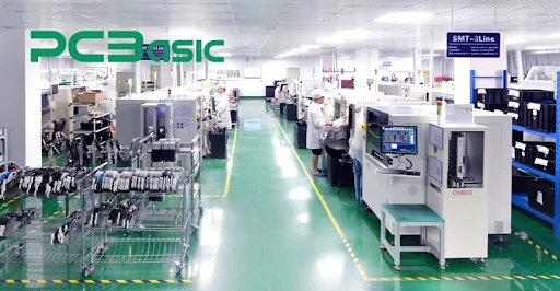
In modern electronics manufacturing, achieving high-quality, reliable circuit boards requires a deep understanding of both PCB fabrication and PCBA assembly workflows. Whether you are an engineer, hardware startup, or OEM brand, knowing how your boards are made helps ensure consistent performance and long-term reliability. At PCBasic, we deliver fully optimized manufacturing solutions using advanced SMT meaning processes and end-to-end engineering support as a professional PCBA service provider. This complete guide walks you through every stage of PCB manufacturing and PCBA assembly inside PCBasic’s smart factory ecosystem.
1. What Is PCB Manufacturing?
Printed Circuit Board (PCB) manufacturing is the process of fabricating the physical board that electrically connects and mechanically supports electronic components. It involves multiple precision steps including imaging, etching, lamination, drilling, plating, and surface finishing. PCBasic follows strict IPC Class standards and integrates digital MES tracking to ensure every PCB meets consistent performance and reliability criteria.
Key Objectives of PCB Manufacturing
• Deliver stable electrical pathways
• Achieve clean signal integrity
• Ensure mechanical strength and long-term durability
• Support high-density and fine-pitch designs for modern electronics
Explore a related post crafted to strengthen your understanding effortlessly.
2. Step-by-Step PCB Manufacturing Process at PCBasic
Step 1: Design Data Review and DFM Check
Before production begins, PCBasic performs a comprehensive DFM (Design for Manufacturability) review. Engineers analyze layer stack-ups, impedance requirements, copper balancing, drill charts, and potential risk points. This prevents manufacturability issues and improves yield during PCBA.
Step 2: PCB Imaging and Pattern Transfer
High-precision LDI (Laser Direct Imaging) transfers the circuit pattern onto copper-clad laminate. This ensures fine-line accuracy for HDI boards, IoT devices, and compact consumer electronics.
Step 3: Etching
Chemical etching removes unwanted copper, leaving behind the conductive traces that route signals across the board.
Step 4: Lamination
For multilayer PCBs, layers are stacked and bonded using heat and pressure. PCBasic supports 4-layer to 32-layer lamination with high-TG materials, FR-4, Rogers, PTFE, hybrid stack-ups, and advanced dielectric materials.
Step 5: Drilling & Laser Microvias
CNC drilling creates through-holes, while UV CO₂ lasers enable microvias for HDI and BGA-dense designs.
Step 6: Plating
Copper plating reinforces vias and ensures strong electrical connections. Advanced through-hole plating minimizes voids and improves reliability.
Step 7: Solder Mask Application
Green, black, white, red, and matte black solder mask options are available. PCBasic uses precision alignment and vacuum exposure to prevent solder bridging in assembly.
Step 8: Silkscreen Printing
Component labels, polarity marks, and logos are printed onto the PCB surface using UV ink technology.
Step 9: Surface Finishing
To protect copper pads and improve solderability, PCBasic offers:
• ENIG
• ENEPIG
• Immersion Tin
• HASL / Lead-Free HASL
• OSP
ENIG/ENEPIG finishes are recommended for high-reliability PCBA builds.
3. What Is PCBA Assembly?
Printed Circuit Board Assembly (PCBA) refers to mounting electronic components onto the fabricated PCB. It combines SMT (Surface Mount Technology), THT (Through-Hole Technology), inspection, testing, and final manufacturing steps that convert a bare PCB into a functional electronic product.
4. PCBasic’s Complete PCBA Assembly Workflow
Step 1: Component Sourcing
PCBasic maintains partnerships with global distributors including DigiKey, Mouser, Arrow, and LCSC. Every component batch undergoes:
• IQC inspection
• Moisture sensitivity management
• Lot traceability through MES
Step 2: SMT Solder Paste Printing
Using 3D SPI inspection, PCBasic ensures correct paste volume and stencil alignment—critical for preventing bridging, tombstoning, and voids.
Step 3: High-Speed SMT Placement
SMT machines place components with up to ±40-micron accuracy, suitable for 01005 passives and 0.25 mm pitch BGAs.
Step 4: Reflow Soldering
Nitrogen reflow ovens ensure clean solder joints with lower oxidation and higher reliability. Temperature profiles are tracked for each work order.
Step 5: AOI / SPI / X-Ray Inspection
PCBasic applies multi-stage inspections:
• SPI for paste height
• AOI for solder joint quality
• X-ray for BGA, QFN, and hidden solder joints
This eliminates early defects before progression to wave soldering or functional test.
Step 6: Through-Hole & Wave Soldering
Selective wave soldering ensures clean THT joints for connectors, power modules, and high-current components.
Step 7: Conformal Coating & Encapsulation (Optional)
For automotive, industrial, and outdoor electronics, PCBasic supports:
• Acrylic / silicone coating
• Potting and resin encapsulation
• Moisture & corrosion protection
Step 8: Functional Testing
PCBasic builds custom fixtures for:
• ICT
• FCT
• Power-on tests
• RF tests
• End-of-line validation
5. Quality Control and Traceability at PCBasic
What sets PCBasic apart is its digital manufacturing ecosystem. All data—including operator records, machine logs, reflow curves, component batches, and AOI images—is traceable through MES/ERP/CRM/IoT platforms.
Quality Certifications
• ISO 9001
• ISO 13485 (Medical)
• IATF 16949 (Automotive)
• IPC-A-610 Class 2 & Class 3
This makes PCBasic a reliable partner for industries requiring extreme precision and low failure rates.
6. Applications PCBasic Serves
PCBasic supports high-mix, small-to-medium batch PCBs and PCBA for:
• IoT hardware
• Industrial control systems
• Consumer electronics
• Robotics and drones
• Medical electronics
• Automotive electronics
• Smart home devices
7. Why PCBasic Is a Trusted Manufacturing Partner
Key Advantages
• High-mix & small-batch specialization
• Transparent quoting & fast turnaround
• Material substitution and engineering support
• Full DFM/DFT reviews
• Strict quality inspections at every stage
• Global shipping to 170+ countries
PCBasic’s combination of engineering depth, advanced equipment, and digital traceability ensures every board meets the highest manufacturing standards.
Conclusion
From PCB fabrication to turnkey PCBA assembly, PCBasic provides a complete, reliable, and engineering-driven manufacturing solution for global hardware teams. By integrating precise PCB production, advanced SMT assembly, strict inspection systems, and full traceability, PCBasic ensures every project—from prototypes to mass production—meets the highest quality and reliability expectations.
If you need a trusted PCB and PCBA partner with strong technical capabilities and fast delivery, PCBasic is ready to support your next hardware project.
Explore deeper ideas crafted to broaden your view and fuel meaningful progress.